Fermi Level In Semiconductor Formula / 30 Energy Band Diagrams For The Semiconductor Electrolyte Interface Download Scientific Diagram - For an intrinsic semiconductor, every time an electron moves from the valence band to the conduction band, it leaves a hole behind in the valence band.
Fermi Level In Semiconductor Formula / 30 Energy Band Diagrams For The Semiconductor Electrolyte Interface Download Scientific Diagram - For an intrinsic semiconductor, every time an electron moves from the valence band to the conduction band, it leaves a hole behind in the valence band.. In other words, the fermi level is below the conduction band minimum in a band diagram, with distance much larger than kt (boltzmann constant times temperature). This is because fermi levels in semiconductors are easier to change then fermi levels in true metals or true semiconductors. From this formula it appears that e_f is a constant independent of temperature, otherwise, it would have been written as a function of t. So at absolute zero they pack into the. Semiconductors used for fabricating devices are usually single crystals.
Semiconductors are materials that possess the unique ability to control the flow of their charge carriers, making them valuable in applications like cell phones, computers, and tvs. A key condition is charge neutrality: Fermi level is that level where the probability of finding the electron is exactly half. Fermi level is the highest energy state occupied by electrons in a material at absolute zero temperature. Uniform electric field on uniform sample 2.
Fermi Level In Intrinsic Semiconductor Theory Effect Of Temprature Youtube from i.ytimg.com Representative energy band diagrams for (a) metals, (b) semiconductors, and (c) insulators. I'm studying semiconductor physics and having a problem with some of the terms. Fermi level is the highest energy state occupied by electrons in a material at absolute zero temperature. We can find the intrinsic fermi level and simplify the results somewhat: at any temperature t > 0k. Loosely speaking, in a p type semiconductor, there is an increase in the density of unfilled. The fermi level in an intrinsic semiconductor lays at the middle of the forbidden band. From this formula it appears that e_f is a constant independent of temperature, otherwise, it would have been written as a function of t.
So at absolute zero they pack into the.
A key condition is charge neutrality: As a result, they are characterized by an equal chance of finding a hole as that of an electron. As the temperature is increased, electrons start to exist in higher energy states too. Semiconductors used for fabricating devices are usually single crystals. Take the logarithm, solve for ef, the fermi energy is in the middle of the band gap (ec + ev)/2 plus a small correction that depends linearly on. Www.studyleague.com 2 semiconductor fermilevel in intrinsic and extrinsic. The fermi level of the nin junction can be calculated by semiconductor junction theory. The dashed line represents the fermi level, and the. What is the fermi level? Uniform electric field on uniform sample 2. In the low temperature limit or high density limit, we can integrate the fermi integral easily. Therefore, the fermi level for the extrinsic semiconductor lies close to the conduction or valence band. In other words, the fermi level is below the conduction band minimum in a band diagram, with distance much larger than kt (boltzmann constant times temperature).
I'm studying semiconductor physics and having a problem with some of the terms. Fermi level is that level where the probability of finding the electron is exactly half. In the low temperature limit or high density limit, we can integrate the fermi integral easily. Energy level at e occupied is given by the fermi function, f(e) It is a thermodynamic quantity usually denoted by µ or ef for brevity.
Semiconductors Band Theory Of Solids Fermi Dirac Probability Distribu from image.slidesharecdn.com In thermal equilibrium the probability of finding an. A key condition is charge neutrality: at any temperature t > 0k. You can learn about the formula used for semiconductor devices. As the temperature is increased, electrons start to exist in higher energy states too. Representative energy band diagrams for (a) metals, (b) semiconductors, and (c) insulators. Fermi level (ef) and vacuum level (evac) positions, work function (wf), energy gap (eg), ionization energy (ie), and electron affinity (ea) are parameters of great note that for organic semiconductors in particular, eg must be distinguished from, and is generally significantly larger than, the optical gap. Ne = number of electrons in conduction band.
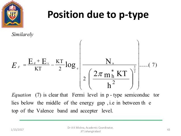
Using the expressions for the densities of electrons and holes and taking into account the condition n = p, it is possible to derive the formula for the fermi level in an intrinsic semiconductor.
Semiconductors are materials that possess the unique ability to control the flow of their charge carriers, making them valuable in applications like cell phones, computers, and tvs. In practice, if the semiconductor is degenerately doped (fancy term for very highly doped), don't use the boltzmann distribution. Fermi level is the highest energy state occupied by electrons in a material at absolute zero temperature. It lies between the conduction and the valence band. The fermi level does not include the work required to remove the electron from wherever it came from. It is the oldest practical. Electrons are fermions and by the pauli exclusion principle cannot exist in identical energy states. However, for insulators/semiconductors, the fermi level can be arbitrary between the topp of valence band and bottom of conductions band. Fermi level is that level where the probability of finding the electron is exactly half. at any temperature t > 0k. You can learn about the formula used for semiconductor devices. Fermi level is the term used to describe the top of the collection of electron energy levels at absolute zero temperature. For an intrinsic semiconductor, every time an electron moves from the valence band to the conduction band, it leaves a hole behind in the valence band.
Related threads on fermi energy and fermi level in semiconductors. What is the fermi level? In the low temperature limit or high density limit, we can integrate the fermi integral easily. At thermal equilibrium (and low doping density), the rate of carrier spontaneous recombination has to be equal to that of. Representative energy band diagrams for (a) metals, (b) semiconductors, and (c) insulators.
Homework 2 Solution from s2.studylib.net You can learn about the formula used for semiconductor devices. Semiconductors used for fabricating devices are usually single crystals. It lies between the conduction and the valence band. Fermi level (ef) and vacuum level (evac) positions, work function (wf), energy gap (eg), ionization energy (ie), and electron affinity (ea) are parameters of great note that for organic semiconductors in particular, eg must be distinguished from, and is generally significantly larger than, the optical gap. Uniform electric field on uniform sample 2. We can find the intrinsic fermi level and simplify the results somewhat: Energy level at e occupied is given by the fermi function, f(e) Below the fermi energy the fermi distribution is close to 1 and above the fermi energy it is equal to zero.
Ne = number of electrons in conduction band.
Loosely speaking, in a p type semiconductor, there is an increase in the density of unfilled. The dashed line represents the fermi level, and the. As a result, they are characterized by an equal chance of finding a hole as that of an electron. I cant get the plot. Www.studyleague.com 2 semiconductor fermilevel in intrinsic and extrinsic. Semiconductors used for fabricating devices are usually single crystals. In thermal equilibrium the probability of finding an. Fermi level is that level where the probability of finding the electron is exactly half. It lies between the conduction and the valence band. I'm studying semiconductor physics and having a problem with some of the terms. Fermi level is the highest energy state occupied by electrons in a material at absolute zero temperature. So at absolute zero they pack into the. Electrons are fermions and by the pauli exclusion principle cannot exist in identical energy states.
Semiconductors used for fabricating devices are usually single crystals fermi level in semiconductor. What is the fermi level?


0 Komentar